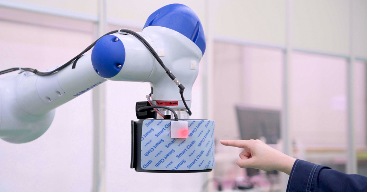
I-PEX株式会社(本社:京都市下京区、代表取締役社長執行役員:小西 玲仁、以下 I-PEX)のグループ会社であるI-PEX Piezo Solutions株式会社(本社:山口県宇部市、代表取締役CEO:緒方 健治、以下 I-PEX Piezo Solutions)は、I-PEX Piezo Solutionsが提供するPt/ZrO₂バッファ層付きSi基板「KRYSTAL® Wafer」を活用し、強相関酸化物であるLaNiO₃薄膜をシリコン基板上に高品質に成長させ、電気的操作によって熱伝導率を可逆的に制御する技術を実現しました。
The co-authored paper summarizing these research results has been published in the scientific journal "Applied Physics Express" (Vol. 19, No. 3, March 2026), published by the Japan Society of Applied Physics.
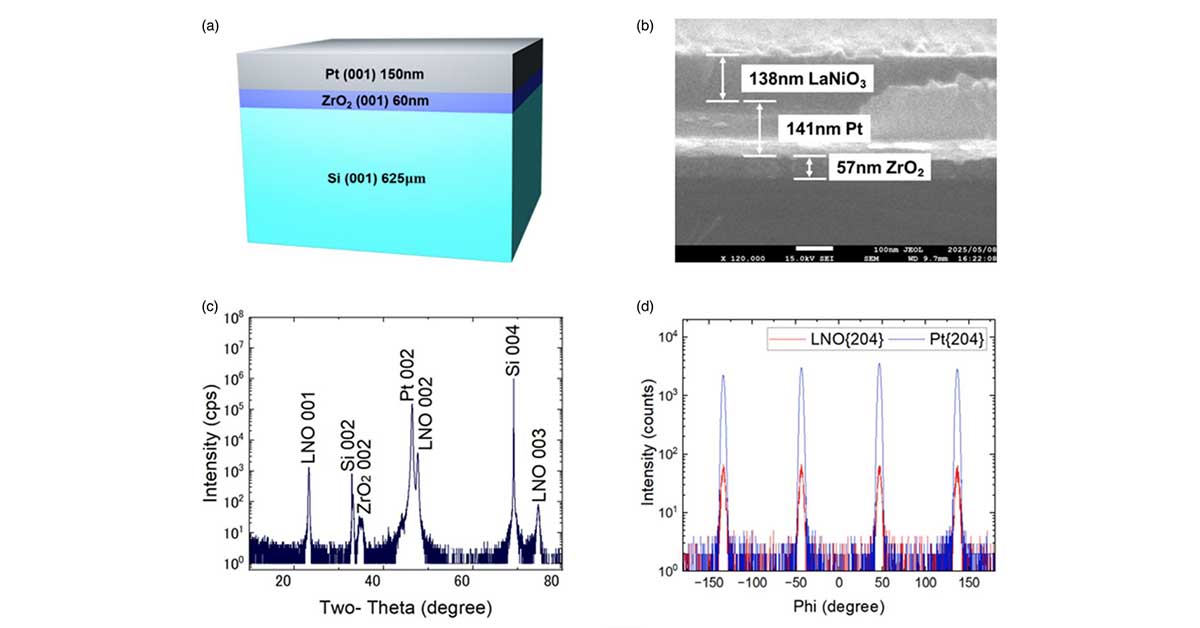
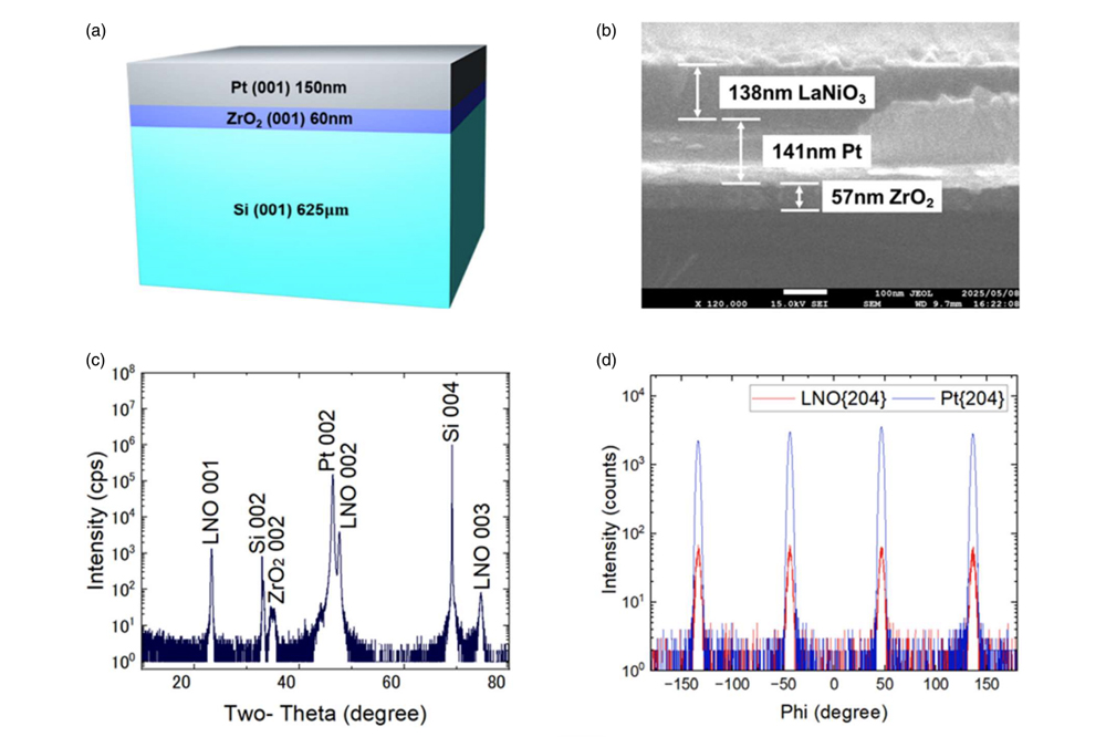 High-quality growth of LaNiO₃ thin films on KRYSTAL® Wafer. (a) Substrate structure. (b) Electron microscope image of a cross-section of the thin film (film thickness approximately 140 nm). (c)(d) X-ray diffraction analysis confirmed that LaNiO₃ was grown on a Si substrate with high crystallinity comparable to that of a single-crystal substrate. (Quoted from the paper)
For more details on the research results and paper, please click here.
Background
The technology of electrically controlling thermal conductivity is a crucial core technology for thermal transistors and thermal management in next-generation electronics. However, conventionally, growing strongly correlated oxides such as LaNiO₃ with high quality required expensive single-crystal substrates such as LSAT and YSZ, posing significant challenges in terms of cost and productivity for industrial applications.
Overview of the Technology
In this study, we successfully achieved epitaxial growth of LaNiO₃ on a conventional Si substrate by using the Pt/ZrO₂ buffer layer of KRYSTAL® Wafer. The crystallinity reached a level comparable to that of single-crystal substrates, and we have experimentally confirmed that high thermal switching performance, previously not expected with on Si substrates, was achieved.
Main features of this technology
- High-quality epitaxial growth on Si substrates: Achieving high-quality growth of LaNiO₃ thin films on Si substrates, the standard substrate in the semiconductor industry, without using expensive single-crystal substrates.
- Reversible control of thermal conductivity: Thermal conductivity can be turned on and off through electrical manipulation, effectively functioning as a thermal transistor.
- Crystallinity comparable to single-crystal substrates: The superior epitaxial growth environment of KRYSTAL® Wafer enables performance on Si substrates that was previously only achievable with expensive substrates.
- High suitability with mass production and practical application: Can be integrated into existing semiconductor manufacturing processes, offering significant business value in terms of cost reduction and scalability.
I-PEX Piezo Solutions株式会社について
I-PEX Piezo Solutions株式会社は、I-PEXグループの圧電MEMS加工部門を独立し、優れた単結晶圧電薄膜の成膜技術と融合する事で、高性能な圧電薄膜の成膜と圧電MEMSの加工技術を持つ、独立系圧電MEMSファウンドリとして設立されました。